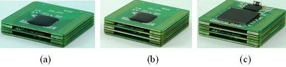
 Figure: a) The MorPack platform; b) The MorPack platform with a discrete cosine transform (DCT) accelerator; c) The MorPack platform with a programmable logic chip (FPGA)
Recently the NARL’s National Chip Implementation Center (CIC) has developed a three-dimension (3D) heterogeneous integration (HI) system platform-Morphing Package (MorPack, see figure) that can cut the development time and cost of multi-chip systems, because it allows for the easy integration of chips with different functions into one tightly-bound package. And it can be applied to develop chips for various electronic devices including communications, security, medicine, recreation gadgets, etc.
The MorPack platform is a stack of sub-modules, which are each composed of bare chips, a fiberglass and copper substrate, connection bridges, and solder balls. It is developed by using the packaging integration technique and the design concept of platform system. The applicable system partition approach is adopted, and tri-state interface used to carry out the connection with the bare die signal of each substrate to make MorPack with optimum system peripheral expandability and flexibility of updating bare die with extremely low cost in accordance with users’ demand. In addition, the application of the packaging integration technique and 3D stacked framework has also made the MorPack platform to possess the capability of heterogeneous chip integration and the character of miniaturization. At present, the MorPACK platform is 4 x 4 centimeters, but the NARL-CIC is researching to downsize it to one fourth, by adopting the flip-chip packaging technology, without compromising existing advantages.
With the MorPack platform, electronics developers can stack up different modules into one chip instead of laying out modules separately, which would occupy too much space on a carrier board, and the performance can also be boosted because the circuits are closer to each other. Therefore, for each IP core-design project, the reusable MorPACK platform can, on average, cut down development time by three to six months and reduce cost by NT$ 1.5 million (ca. $51,000). Currently, seven research groups at six universities have already adopted the MorPACK platform to develop IP cores needed by intelligent systems for biomedical, 3D communication, image processing and other applications.