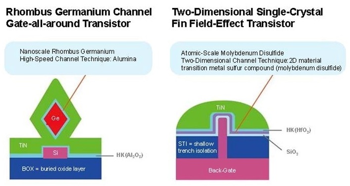
Figure 1. Ge (germanium), TiN (titanium nitride), Si (silicon), HfO2 (hafnium oxide), SiO2 (silica).
Everything Began with Moore's Law
According to Moore's Law, which is well-known in the semiconductor field, the amount of transistors on an integrated circuit (IC) is expected to double every 18 to 24 months. In other words, as the transistor's size shrinks, the channels of current within the transistors also decrease in channel width. Currently, the most advanced IC mass production techniques enable the manufacturing of ICs with 14-nanometer-wide channels (commonly known as the 14 nanometer technology node). However, researchers have begun to study ICs with 5-nanometer-wide channels. This width approximates the physical li
The motivation for decreasing the scale of a transistor is to shorten the channel length, thereby reducing the time and energy required for current transportation. Advances in miniaturization enable calculation speed and energy saving. Therefore, having experienced difficulties in miniaturizing channel lengths in silicon, scientists have attempted to seek alternative methods, such as the substitution of silicon with alternate materials and the heterogeneous integration of materials, which accelerate electron movement through the modified channels.
Various structural modifications can also be applied to a fin field-effect transistor (FinFET)2 . This enables creating additional current channels in the same space or enhancing control over electrical currents and reducing current leakage, thus enhancing component efficiency. These alternative techniques are distinct from conventional silicon-ba
Nanoscale Rhombus Germanium High-Speed Channel Technique
The material characteristics of germanium are similar to those of silicon. Compared with silicon, germanium enables faster electron transmission speed through its various crystal planes. Thus, germanium is considered by scientists as the first primary material to be mass produced in the postsilicon era.
NDL adopted an accurate nano-etching technique to carve an innovative rhombus channel structure that functions as a FinFET even though it is only a few tens of nanometers in size. A nanoscale rhombus germanium channel structure was created from a germanium channel. Electrical current can move each edge of a rhombus shaped channel; three contact surfaces exist between the gate and the current channel in this FinFET, resulting in three current channels. The current channels on the three sides of this FinFET can be expanded to four high-speed transmission faces (Figure 1). The defects on the channel interface were removed during the manufacturing process, thereby decreasing the electrical energy consumed in component operations. This increased the current transmission speed by 100%, substantially enhancing the transistor properties.
Atomic-Scale Molybdenum Disulfide Two-Dimensional Channel Technique
Molybdenum disulfide is a novel material that has received attention in recent years and has been examined by the academia and industry. It is manufactured as an ultrathin 2D material, which is then heterogeneously integrated with conventional silicon materials. However, current techniques only enable integrating 2D molybdenum disulfide with planar transistors. NDL was the first to integrate a 4-nanometer-thick (six layers of molybdenum disulfide molecules) molybdenum disulfide material with a pre-existing FinFET to develop the world's first FinFET component that features a 2D molybdenum disulfide channel (Figure 1) and a unique back-gate control design. This double-gate approach decreases leakage current, thus reducing the energy consumption by half.
This 2D material was created through a vapor deposition method, which has been applied by relevant industries for many years. The method enables integrating innovative materials with conventional semiconductor manufacturing processes to provide a feasible approach for component circuit designs for the next generation of IC technology. Therefore, this component has received the attention of scientists worldwide.
Among the World's Leading Institutions: Establishment of a Foundation for Researching and Developing Prospect Components
At the 2015 IEDM, NDL (6 papers) was among the world's leading institutions in semiconductor science, along with the Interuniversity Micro Electronics Center (20 papers), International Business Machines Corporation (10 papers), Taiwan Semiconductor Manufacturing Company (7 papers), and Intel (5 papers). NDL has achieved major breakthrough in related research and is expected to establish an essential foundation of knowledge for the postsilicon era; relevant domestic academic and industrial institutions are expected to apply this knowledge to create service platforms for researching and developing prospective components. Through continual improvement in technology, the institution can cultivate highly professional talents with master's and doctoral degrees, who can engage in industrial research fields, such as smart technology, green energy, and intelligent manufacturing, to sustain the competitiveness of the domestic semiconductor industry.
NDL focuses on the research and development of prospective semiconductor components to establish open research service platforms for linking domestic academia and industries with international counterparts. For many years, NDL has provided research and development services to apply its globally recognized research achievements to various manufacturing research and development platforms. These platforms facilitate the commercialization and small-scale production of research products formulated in academia. NDL has established interdisciplinary practical learning platforms (involving nonconventional electronics and electromechanical fields such as microelectronics, physics, chemistry, optoelectronics, microelectromechanical engineering, and mechanics) to supplement interdisciplinary studies with practical achievements. This enables highly professional personnel with master's and doctoral degrees to apply their hard-earned knowledge immediately as they enter the workplace, thereby decreasing the barriers of interdisciplinary technology integration and the time expended on personnel training. NDL has been operating for more than 20 years. Numerous personnel with master's and doctoral degrees have received training in the institution and become essential executive managers in relevant industries; hence, NDL has contributed greatly to the domestic semiconductor industry.
1. IEDM is perceived as the Olympics of the field of semiconductor nanocomponents. At this marquee international meeting, major industrial and academic semiconductor institutions, including Taiwan Semiconductor Manufacturing Company, Macronix, Intel, Samsung, Interuniversity Micro Electronics Center, CEA-LETI, and NDL, published the latest techniques related to semiconductor manufacturing and electronic components.
2. A field-effect transistor is an electronic component that controls electrical current. It is usually analogized as a water reservoir, in which the water supply, water outlet, and water flow control correspond to the source (S), drain (D), and gate (G) of the component, respectively. In a conventional field-effect transistor, the gate only controls one side of the current channel (as shown in the left figure). When the gate length is reduced to nanometer scale, a conventional gate ineffectively modulates electrical currents. The FinFET improves on the conventional field-effect transistor design. In a FinFET, the gate features a fin-like three-dimensional structure (as shown in the right figure) and controls the top, left, and right sides of the current channel. This facilitates contracting the gate and substantially reducing current leakage.