 (From left) Wen-Hwa Chen, the president of the National Applied Research Laboratories (NARL); Simon M. Sze, the academician of the Academia Sinica; Lih. J. Chen, the deputy minister of the National Science Council; and Fu-Liang Yang, the director general of the NARL's National Nano Device Laboratories together witnessed a new milestone for the development of nano-device technology in Taiwan.
The size is a driving force for the semiconductor industry. In this line of endeavor, the NARL's National Nano Device Laboratory (NDL) has developed a new technology to produce the world's first functional 16-nm SRAM (static random access memory) cell (the lower left image). By adopting this new technology, more than 15 billion transistors can be accommodated in an area of 1 cm2 on a microchip. This is 10 times more than the conventional microchip produced by the 45-nm technology. With this new technology, size and power consumption of microchip can be tremendously reduced. This implies electronic gadgets like cell phones and laptops could become smaller, lighter and cheaper. This achievement was presented at the International Electron Devices Meeting (IEDM), the world's premier forum for leading-edge research into electronic, microelectronic, and nanoelectronic devices and processes, held in Baltimore, Maryland, USA on December 9, 2009 and selected as one of the five late news papers. Besides, this outstanding work has been reported by several well-known international digital media such as EE Times, IEEE Spectrum and Nikkei BP (Business Publications).
The production of nano-devices in Taiwan's semiconductor industry for the govement's "Two Trillion Twin Star Program" will soon advance from the current 45-nm generation to the 32-nm generation. Meanwhile the research and development (R&D) for the 22-nm technology is on-going. Nonetheless, the most advanced 16-nm technology will face several challenges such as physical characteristics and equipment development for production that need to be overcome.
It is estimated that the cost for developing 16-nm technology will be more than 1 billion USD and for scaling-up production 50 billion USD. Therefore, R&Ds are imperative for lowering the capital bottleneck as well as the investment risk. Moreover, breakthroughs in production processes and device performances are crucial to make the commercialization of the 16-nm technology feasible.
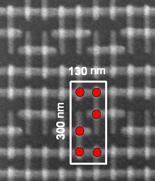 The world's first functional 16-nm SRAM (static random access memory) cell.
At IEDM 2009, the NARL-NDL has presented three key 16-nm technologies: Nano-Injection Lithography; 320℃ Low-Temperature Microwave Activation; and Study of N-Type Germanium Device. The nano-injection lithography is a cheaper way to make the desired pattes. It gets away with expensive masks and a light-sensitive material, photoresist, to create pattes. Apart from saving money, this in tu will eliminate interference problem often encountered when using photoresist. The new process with the 16-nm technology requires only simple equipment to overcome the physical limit of around 10 nm in traditional lithography. With this new technology, an ultimate device size of 5 nm can be realized. This is a major breakthrough for the advanced integrated circuit (IC) process.
The 320℃ low-temperature microwave activation utilizes microwave to significantly lower the conventional annealing temperature of 900℃ to 320℃. This low-temperature activation process is expected to be the key technology for making stack IC devices in the future, similar to building construction. The concept of stacking will be adopted to reduce the size of the chip, hence making electronic product like cell phones and laptops lighter and smaller.
The study of N-type germanium device seeks to replace the conventional silicon with a chemical element, germanium, to pROVide faster and better performance for the 16-nm devices. In this study, a new process was developed to further impROVe the carrier mobility in germanium transistor. This new process will play an important role in the development of low-power-consumption devices.
Among the semiconductor devices, non-volatile memory, i.e., USB and solid-state disks, shows fastest growth in the current market. Nevertheless, devices adopting the 16-nm technology or below will face several challenges. In this connection, the "nano silicon quantum dot energy-saving storage device" developed by the NARL-NDL is the world's first energy-saving storage device that manipulates directly electric field to store data to nano silicon quantum dot. Since electric current is not needed for data storage, the device has extremely low power consumption. This device is expected to have a great potential in the non-volatile memory market. Because of this, the image of the device has been placed on the cover page of Applied Physics Letters published on October 5, 2009.
"The development of the 16-nm technology will determine whether or not Taiwan still maintains its competitive position for the 22-nm generation in the global semiconductor industry," said Fu-Liang Yang, the director general of the NARL-NDL. Taiwan's economics focus and manufacturing capability in the past have rendered the country to be in a good competitiveness status for the global semiconductor industry. To remain so in the future, however, innovative ideas and solid R&D outputs related to the 16-nm technology must be advanced and integrated for the industry. The aforementioned achievements by the NARL-NDL staff in the past year have convinced Dr. Yang that Taiwan is heading toward that direction and the NARL-NDL shall be the global center for nano device research. He hopes that the core technologies developed by the NARL-NDL can serve as the foundation for organizing a research consortium next year. This allows combining resources in industry, govement and academia for the development of the 16-nm technology in Taiwan.